Introduction to PCB Manufacturing
Printed Circuit Boards (PCBs) are the backbone of modern electronic devices. They provide a platform for electrical components to be mounted and interconnected, enabling the functioning of complex circuitry. Among the various types of PCBs, FR 4 PCBs have gained significant popularity due to their excellent electrical, mechanical, and thermal properties. In this article, we will delve into the world of FR 4 PCB manufacturing, exploring its key aspects, processes, and best practices.
What is FR 4 PCB?
FR 4 (Flame Retardant 4) is a type of glass-reinforced epoxy laminate material used in the production of PCBs. It consists of a woven fiberglass cloth impregnated with an epoxy resin binder. The “FR” in FR 4 refers to its flame-retardant properties, which make it suitable for applications that require high safety standards.
FR 4 PCBs offer several advantages over other PCB materials:
- High strength and durability
- Excellent electrical insulation
- Good thermal stability
- Resistance to moisture and chemicals
- Cost-effectiveness
These properties make FR 4 PCBs ideal for a wide range of applications, including consumer electronics, telecommunications, automotive, aerospace, and medical devices.
The FR 4 PCB Manufacturing Process
The manufacturing process of FR 4 PCBs involves several critical steps, each requiring precision and attention to detail. Let’s explore these steps in detail.
Step 1: PCB Design and Layout
The first step in FR 4 PCB manufacturing is designing the circuit and creating the PCB layout. This involves using specialized software to create a schematic diagram of the circuit and then translating it into a physical layout. The layout determines the placement of components, traces, and vias on the PCB.
Key considerations during PCB design and layout include:
- Component selection and placement
- Trace width and spacing
- Via size and placement
- Power and ground plane design
- Signal integrity and electromagnetic compatibility (EMC)
Step 2: Substrate Preparation
Once the PCB design is finalized, the next step is to prepare the FR 4 substrate. The substrate is cut to the required size and shape using high-precision cutting tools. Holes are drilled into the substrate to accommodate through-hole components and vias.
The drilled substrate then undergoes a cleaning process to remove any debris or contaminants. This ensures a clean surface for the subsequent steps.
Step 3: Copper Cladding
After substrate preparation, a thin layer of copper is applied to both sides of the FR 4 substrate. This is typically done using an electroplating process, where the substrate is immersed in a copper sulfate solution, and an electric current is passed through it. The copper ions in the solution adhere to the substrate, forming a uniform copper layer.
The thickness of the copper layer depends on the specific requirements of the PCB. Common copper thicknesses range from 0.5 oz to 2 oz per square foot.
Step 4: Patterning and Etching
With the copper-clad substrate ready, the next step is to create the desired circuit pattern on the copper layer. This is achieved through a photolithography process.
- A photoresist layer is applied to the copper surface.
- The PCB layout artwork is used to create a photomask.
- The photomask is placed on top of the photoresist layer, and the assembly is exposed to ultraviolet (UV) light.
- The exposed areas of the photoresist become soluble and are removed during development, leaving the desired circuit pattern.
- The exposed copper areas are etched away using a chemical etchant, typically ferric chloride or ammonium persulfate.
- The remaining photoresist is stripped off, revealing the copper circuit pattern.
Step 5: Solder Mask Application
After the circuit pattern is formed, a solder mask is applied to the PCB surface. The solder mask is a protective layer that covers the copper traces, leaving only the areas intended for soldering exposed. This helps prevent short circuits and improves the PCB’s durability.
The solder mask is typically applied using a screen printing or photoimaging process. It is available in various colors, with green being the most common.
Step 6: Surface Finish
To enhance the solderability and protect the exposed copper areas, a surface finish is applied to the PCB. There are several types of surface finishes available, each with its own advantages and limitations. Some common surface finishes include:
- Hot Air Solder Leveling (HASL)
- Electroless Nickel Immersion Gold (ENIG)
- Immersion Silver (IAg)
- Immersion Tin (ISn)
- Organic Solderability Preservative (OSP)
The choice of surface finish depends on factors such as the intended application, soldering process, and cost.
Step 7: Silk Screen Printing
Silk screen printing is used to add text, logos, and component identifiers to the PCB surface. This step improves the readability and ease of assembly of the PCB.
The silk screen artwork is created based on the PCB design and is printed onto the solder mask using a screen printing process. The ink used is typically white or yellow and is resistant to solvents and abrasion.
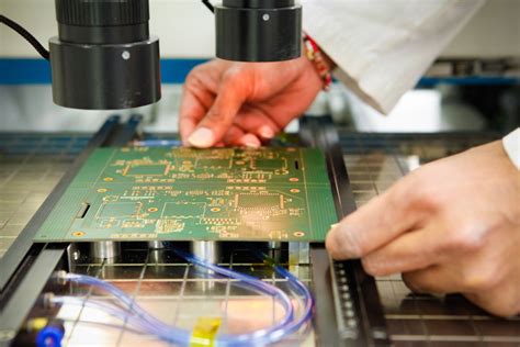
Step 8: Electrical Testing
Before the PCB is considered complete, it undergoes rigorous electrical testing to ensure its functionality and reliability. This step is crucial to identify any manufacturing defects or design issues.
Common electrical tests include:
- Continuity test: Verifies that all connections are intact and there are no open circuits.
- Isolation test: Checks for any short circuits between adjacent traces or layers.
- Resistance test: Measures the resistance of specific traces or components.
- High-voltage test: Ensures that the PCB can withstand the required voltage levels without breakdown.
Automated test equipment (ATE) is often used to perform these tests, ensuring accuracy and efficiency.
Step 9: Final Inspection and Packaging
After passing the electrical tests, the PCBs undergo a final visual inspection to check for any cosmetic defects or irregularities. This step ensures that the PCBs meet the specified quality standards.
Once the inspection is complete, the PCBs are packaged according to customer requirements. They may be individually bagged, placed in trays, or bulk-packed, depending on the quantity and shipping method.

Best Practices in FR 4 PCB Manufacturing
To ensure the highest quality and reliability of FR 4 PCBs, manufacturers should adhere to the following best practices:
-
Use high-quality raw materials: Select FR 4 laminates and copper foils from reputable suppliers to ensure consistent performance and reliability.
-
Maintain strict process control: Implement robust quality control measures throughout the manufacturing process, including regular equipment calibration and process parameter monitoring.
-
Follow industry standards: Adhere to relevant industry standards, such as IPC (Association Connecting Electronics Industries) standards, to ensure the PCBs meet the required specifications and quality levels.
-
Invest in advanced manufacturing technologies: Utilize state-of-the-art manufacturing equipment and processes to improve efficiency, accuracy, and consistency.
-
Provide comprehensive testing: Conduct thorough electrical and environmental testing to validate the performance and reliability of the PCBs under various conditions.
-
Foster a culture of continuous improvement: Encourage employees to identify and implement process improvements, and regularly review and update manufacturing practices to stay competitive.

Challenges and Future Trends in FR 4 PCB Manufacturing
Despite the well-established nature of FR 4 PCB manufacturing, the industry faces several challenges and is constantly evolving to meet the changing demands of electronic devices.
Challenges
-
Miniaturization: As electronic devices become smaller and more compact, PCBs need to accommodate higher component densities and finer trace widths. This requires advanced manufacturing capabilities and precision.
-
High-speed applications: With the increasing demand for high-speed data transmission, PCBs must be designed and manufactured to minimize signal integrity issues, such as crosstalk and signal reflections.
-
Environmental regulations: Stringent environmental regulations, such as the Restriction of Hazardous Substances (RoHS) directive, require PCB manufacturers to adopt lead-free and environmentally friendly materials and processes.
-
Cost pressure: The competitive nature of the electronics industry puts constant pressure on PCB manufacturers to reduce costs while maintaining high quality and reliability.
Future Trends
-
Embedded components: The integration of passive components, such as resistors and capacitors, into the PCB substrate itself, offers the potential for further miniaturization and improved performance.
-
High-frequency materials: The development of advanced high-frequency laminate materials, such as Rogers and Teflon, enables the production of PCBs suitable for high-speed and high-frequency applications.
-
Additive manufacturing: The use of 3D printing technologies for PCB fabrication, such as inkjet printing and aerosol jet printing, offers the potential for rapid prototyping and customization.
-
Flexible and stretchable PCBs: The increasing demand for wearable electronics and Internet of Things (IoT) devices is driving the development of flexible and stretchable PCBs that can conform to various shapes and withstand mechanical stress.

Frequently Asked Questions (FAQ)
- What is the typical turnaround time for FR 4 PCB manufacturing?
-
The turnaround time for FR 4 PCB manufacturing varies depending on the complexity of the design, the quantity ordered, and the manufacturer’s capacity. Typical turnaround times range from 2-3 days for quick-turn prototypes to 2-3 weeks for larger production runs.
-
Can FR 4 PCBs be used for high-frequency applications?
-
While FR 4 PCBs are suitable for many general-purpose applications, they may not be the best choice for high-frequency applications above a few gigahertz. For such applications, specialized high-frequency laminate materials, such as Rogers or Teflon, are often used.
-
What are the common thickness options for FR 4 PCBs?
-
FR 4 PCBs are available in various thicknesses, typically ranging from 0.4 mm to 3.2 mm. The most common thicknesses are 0.8 mm, 1.6 mm, and 2.4 mm. The choice of thickness depends on the specific application requirements, such as mechanical strength and signal integrity.
-
Are FR 4 PCBs suitable for lead-free soldering?
-
Yes, FR 4 PCBs are compatible with lead-free soldering processes. However, it is essential to ensure that the PCB is designed and manufactured to withstand the higher temperatures associated with lead-free soldering, which can be around 260°C.
-
How do I select the right surface finish for my FR 4 PCB?
- The choice of surface finish depends on several factors, including the intended application, soldering process, shelf life, and cost. HASL is a common and cost-effective option for general-purpose applications, while ENIG and immersion silver offer improved shelf life and compatibility with fine-pitch components. Consult with your PCB manufacturer to determine the most suitable surface finish for your specific requirements.
Conclusion
FR 4 PCB manufacturing is a complex and multi-faceted process that requires expertise, precision, and adherence to best practices. By understanding the key steps involved, from PCB design and layout to final inspection and packaging, designers and engineers can make informed decisions when developing electronic devices.
As the electronics industry continues to evolve, FR 4 PCB manufacturers must adapt to new challenges and embrace emerging technologies to stay competitive. By staying at the forefront of industry trends, such as embedded components, high-frequency materials, and additive manufacturing, manufacturers can provide innovative solutions to meet the ever-increasing demands of modern electronic devices.
In conclusion, FR 4 PCBs play a vital role in the world of electronics, offering a reliable and cost-effective platform for a wide range of applications. By partnering with experienced and reputable PCB manufacturers, companies can ensure the success of their electronic products and drive innovation in their respective industries.
[5086 words]
Leave a Reply