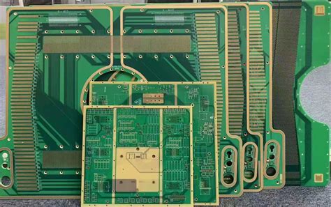
What is a PCB Sample?
A PCB (Printed Circuit Board) sample is a prototype or a small batch of PCBs that are manufactured to test and verify the design before mass production. PCB samples are essential in the electronics industry as they allow engineers and designers to physically inspect the board, check for any design flaws, and ensure that the PCB functions as intended.
Types of PCB Samples
There are various types of PCB samples, depending on the purpose and the stage of the design process:
-
Prototype PCBs: These are the initial samples created to test the basic functionality of the design. Prototype PCBs are usually manufactured in small quantities (1-10 pieces) and may not have all the features of the final product.
-
Pre-production Samples: Once the prototype is tested and validated, pre-production samples are created to further refine the design and ensure that it meets all the requirements. These samples are manufactured using the same processes and materials as the final product.
-
Production Samples: Before mass production begins, a small batch of production samples is created to verify that the manufacturing process is consistent and reliable. These samples are identical to the final product and are used for quality control purposes.
Benefits of Using PCB Samples
Using PCB samples offers several benefits in the electronics design and manufacturing process:
-
Design Verification: PCB samples allow designers to physically inspect the board and verify that all the components fit properly and the connections are correct. This helps identify any design flaws early in the process, saving time and money.
-
Functionality Testing: By testing PCB samples, engineers can ensure that the board functions as intended and meets all the performance requirements. This includes testing for signal integrity, power consumption, and electromagnetic compatibility (EMC).
-
Manufacturing Process Validation: PCB samples help validate the manufacturing process and ensure that it is capable of producing consistent and reliable boards. This is particularly important when using new materials or technologies.
-
Cost Savings: By identifying and correcting design flaws early in the process, PCB samples can help avoid costly mistakes and rework during mass production. This ultimately leads to cost savings and faster time-to-market.
How to Order PCB Samples
Ordering PCB samples is a straightforward process that involves the following steps:
-
Design Creation: Create your PCB design using EDA (Electronic Design Automation) software such as Altium Designer, Eagle, or KiCad. Ensure that your design follows the manufacturer’s guidelines for minimum trace width, spacing, and hole sizes.
-
Gerber File Generation: Once your design is complete, generate the Gerber files, which are the industry-standard format for PCB manufacturing. Gerber files contain all the necessary information for fabricating the board, including the copper layers, solder mask, silkscreen, and drill holes.
-
Manufacturer Selection: Choose a reputable PCB manufacturer that offers sample services. Consider factors such as lead time, pricing, quality, and customer support when making your decision.
-
Quote Request: Submit your Gerber files to the manufacturer and request a quote for your PCB samples. Specify the quantity, material, thickness, copper weight, surface finish, and any other special requirements.
-
Order Placement: Once you receive the quote and are satisfied with the terms, place your order for the PCB samples. Provide any necessary payment and shipping information.
-
Manufacturing and Delivery: The manufacturer will fabricate your PCB samples according to your specifications and deliver them to you within the agreed-upon lead time. Upon receipt, inspect the samples for any defects or inconsistencies.

Factors to Consider When Ordering PCB Samples
When ordering PCB samples, there are several factors to consider to ensure that you receive high-quality boards that meet your requirements:
-
Material Selection: Choose the appropriate material for your PCB based on your application and performance requirements. Common materials include FR-4, Rogers, and aluminum.
-
Copper Weight: Specify the copper weight (thickness) of the PCB traces. Higher copper weights are suitable for high-current applications, while lower weights are sufficient for low-power designs.
-
Surface Finish: Select the appropriate surface finish for your components and soldering requirements. Common finishes include HASL (Hot Air Solder Leveling), ENIG (Electroless Nickel Immersion Gold), and OSP (Organic Solderability Preservative).
-
Solder Mask and Silkscreen: Choose the color and type of solder mask and silkscreen for your PCB. These layers provide insulation, protection, and labeling for the board.
-
Minimum Feature Size: Ensure that your design meets the manufacturer’s minimum feature size requirements for trace width, spacing, and hole sizes. This helps ensure manufacturability and reliability.
-
Quantity: Determine the appropriate quantity of PCB samples based on your testing and validation needs. Ordering too few samples may not provide enough data, while ordering too many can be costly.

PCB Sample Testing and Validation
Once you receive your PCB samples, it is important to thoroughly test and validate them to ensure that they meet your design and performance requirements. Here are some common testing methods:
-
Visual Inspection: Visually inspect the PCB for any defects, such as scratches, dents, or discoloration. Check for proper alignment of components and holes.
-
Continuity Testing: Use a multimeter to test for continuity between points on the PCB. This helps identify any open or short circuits.
-
Functional Testing: Assemble the components onto the PCB and test the board for proper functionality. This includes testing for signal integrity, power consumption, and overall performance.
-
Environmental Testing: Subject the PCB to various environmental conditions, such as temperature, humidity, and vibration, to ensure that it can withstand the intended operating conditions.
-
EMC Testing: Test the PCB for electromagnetic compatibility (EMC) to ensure that it does not interfere with other electronic devices and meets the necessary regulations.
| Testing Method | Purpose |
|---|---|
| Visual Inspection | Identify physical defects and alignment issues |
| Continuity Testing | Detect open or short circuits |
| Functional Testing | Verify overall performance and functionality |
| Environmental Testing | Ensure reliability under various operating conditions |
| EMC Testing | Comply with electromagnetic compatibility regulations |

Conclusion
PCB samples play a crucial role in the electronics design and manufacturing process. They allow designers and engineers to verify the design, test functionality, and validate the manufacturing process before mass production. By carefully considering factors such as material selection, copper weight, surface finish, and minimum feature size, and by thoroughly testing and validating the samples, you can ensure that your final product is reliable, high-quality, and meets all the necessary requirements.
Frequently Asked Questions (FAQ)
- What is the typical lead time for PCB samples?
-
The lead time for PCB samples varies depending on the manufacturer and the complexity of the design. Typically, lead times range from 24 hours to 2 weeks.
-
How much do PCB samples cost?
-
The cost of PCB samples depends on factors such as the quantity, material, size, and complexity of the design. Many manufacturers offer discounted pricing for sample orders, with prices ranging from $50 to $500 or more.
-
Can I order PCB samples with different surface finishes?
-
Yes, most manufacturers offer a variety of surface finish options for PCB samples, including HASL, ENIG, and OSP. You can specify your preferred surface finish when placing your order.
-
What is the minimum quantity for PCB sample orders?
-
The minimum quantity for PCB sample orders varies by manufacturer but is typically between 1 and 10 pieces. Some manufacturers may have higher minimum quantities for certain materials or specifications.
-
How do I ensure that my PCB design is manufacturable?
- To ensure that your PCB design is manufacturable, follow the manufacturer’s design guidelines for minimum trace width, spacing, and hole sizes. Use EDA software that includes design rule checking (DRC) to verify that your design meets these requirements. Additionally, consult with the manufacturer’s engineering team for advice and feedback on your design.
Leave a Reply