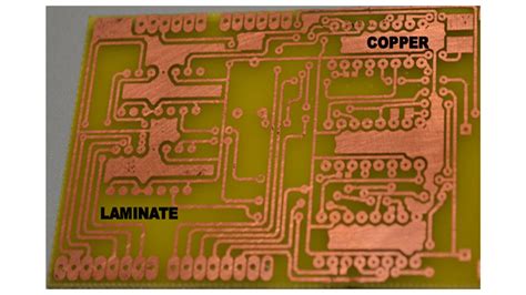
What is PCB Lamination?
PCB lamination is a crucial step in the manufacturing process of printed circuit boards (PCBs). It involves bonding together multiple layers of materials, such as copper foil, prepreg, and core laminates, using heat and pressure to create a single, solid board. The lamination process ensures that the PCB has the necessary mechanical strength, electrical insulation, and thermal stability to function properly in various electronic applications.
The Importance of PCB Lamination
PCB lamination plays a vital role in the overall performance and reliability of the final product. Some of the key reasons why lamination is essential include:
-
Mechanical Strength: Lamination bonds the layers together, creating a strong and durable PCB that can withstand physical stress and vibrations.
-
Electrical Insulation: The lamination process ensures proper insulation between conductive layers, preventing short circuits and signal interference.
-
Thermal Stability: Laminated PCBs have better thermal stability, allowing them to operate in a wide range of temperatures without warping or delaminating.
-
Moisture Resistance: Lamination helps protect the PCB from moisture, which can cause corrosion and other issues that affect the board’s performance.
The PCB Lamination Process
The PCB lamination process typically involves the following steps:
1. Material Preparation
Before lamination, the PCB materials must be prepared. This includes:
- Cutting the core laminates and prepreg to the desired size
- Cleaning the copper foil to remove any contaminants
- Applying a thin layer of oxide to the copper foil to improve adhesion
2. Layup
The layup process involves stacking the prepared materials in a specific order, based on the PCB design. A typical layup consists of:
- Core laminates
- Prepreg
- Copper foil
The number of layers and their arrangement may vary depending on the complexity of the PCB design.
3. Lamination Press
Once the layup is complete, the stack is placed in a lamination press. The press applies heat and pressure to the stack, causing the prepreg to melt and flow, bonding the layers together. The typical lamination process involves:
- Preheating the stack to remove any moisture
- Applying pressure and heat (usually between 180-200°C) for a specific duration
- Cooling the laminated PCB under pressure to prevent warping
| Parameter | Value |
|---|---|
| Temperature | 180-200°C |
| Pressure | 200-400 psi |
| Duration | 1-2 hours |
4. Post-Lamination Processing
After lamination, the PCB undergoes several post-processing steps, including:
- Trimming the edges to remove any excess material
- Drilling holes for vias and component mounting
- Surface finishing, such as solder mask application and silkscreen printing

Factors Affecting PCB Lamination Quality
Several factors can impact the quality of the laminated PCB, including:
-
Material Selection: Choosing the right materials, such as high-quality prepreg and core laminates, is crucial for achieving a strong and reliable lamination.
-
Layup Accuracy: Proper alignment of the layers during the layup process is essential to ensure the PCB’s structural integrity and prevent issues like signal interference.
-
Lamination Parameters: The temperature, pressure, and duration of the lamination process must be carefully controlled to achieve optimal bonding without damaging the materials.
-
Cleanliness: Contaminants on the copper foil or other materials can weaken the bond and cause delamination. Ensuring a clean environment and proper handling of materials is essential.

Advanced PCB Lamination Techniques
As PCB designs become more complex and demanding, advanced lamination techniques have been developed to address specific challenges, such as:
-
Sequential Lamination: This technique involves laminating multiple sub-assemblies separately and then laminating them together to form the final PCB. This allows for greater design flexibility and improved signal integrity in high-speed applications.
-
Buried and Blind Vias: Lamination processes have been adapted to accommodate buried and blind vias, which are used to interconnect internal layers without being visible on the surface of the PCB. This technique enables higher density designs and improved signal routing.
-
Thermally Conductive Laminates: For applications that generate significant heat, thermally conductive laminates can be used to improve heat dissipation and prevent thermal damage to the PCB and its components.

The Benefits of Working with RAYPCB for PCB Lamination
RAYPCB is a leading provider of high-quality PCB lamination services, offering a range of benefits to its clients, including:
-
State-of-the-Art Equipment: RAYPCB invests in the latest lamination equipment and technologies to ensure consistent, reliable results.
-
Experienced Technicians: Our team of skilled technicians has extensive experience in PCB lamination, ensuring that every project is handled with expertise and attention to detail.
-
Strict Quality Control: We adhere to stringent quality control measures throughout the lamination process to guarantee the highest standards of workmanship.
-
Rapid Turnaround: RAYPCB offers fast turnaround times without compromising on quality, helping you meet tight deadlines and get your products to market quickly.
-
Customization Options: We work closely with our clients to understand their specific requirements and offer customized lamination solutions to meet their unique needs.
Frequently Asked Questions (FAQ)
-
Q: What is the difference between prepreg and core laminates?
A: Prepreg is a partially cured material that contains a resin and reinforcement fabric, while core laminates are fully cured materials that provide structural support to the PCB. Prepreg melts and flows during lamination, bonding the layers together, while core laminates maintain their solid state. -
Q: Can PCB lamination be done in-house?
A: While it is possible to perform PCB lamination in-house, it requires significant investment in equipment, materials, and skilled personnel. Outsourcing lamination to a professional provider like RAYPCB ensures consistent, high-quality results and allows you to focus on your core competencies. -
Q: How does the number of layers affect the lamination process?
A: As the number of layers in a PCB increases, the lamination process becomes more complex. More layers require more precise alignment, longer press cycles, and greater attention to detail to ensure proper bonding and prevent issues like delamination or warping. -
Q: What is the typical turnaround time for PCB lamination?
A: The turnaround time for PCB lamination depends on various factors, such as the complexity of the design, the number of layers, and the workload of the lamination service provider. At RAYPCB, we strive to offer fast turnaround times without compromising on quality, with typical lead times ranging from 24 to 48 hours. -
Q: How can I ensure the best results when outsourcing PCB lamination?
A: To ensure the best results when outsourcing PCB lamination, choose a reputable provider like RAYPCB with a proven track record of quality and reliability. Provide clear and accurate specifications for your project, including material requirements, layer stackup, and any special considerations. Maintain open communication with your provider throughout the process to address any concerns or questions promptly.
In conclusion, PCB lamination is a critical step in the manufacturing process that directly impacts the performance, reliability, and durability of the final product. By understanding the lamination process, the factors that affect its quality, and the benefits of working with a trusted provider like RAYPCB, you can ensure that your PCBs meet the highest standards and deliver optimal results in your electronic applications.
Leave a Reply