How PCB Panelization Works
The panelization process typically follows these steps:
- Individual PCB designs are created in CAD software
- The separate designs are arranged in an optimized layout on a larger manufacturing panel
- Tooling holes, fiducials, test coupons, and break-off tabs are added to the panel
- The combined panelized design is sent for fabrication
- After manufacturing, the individual boards are depanelized by breaking them out of the larger panel
PCB Panel Sizes and Specifications
Standard PCB manufacturing panels come in a few common sizes:
| Panel Size | Dimensions (mm) | # of Boards (50x50mm) |
|---|---|---|
| Small | 229 x 279 | 20 |
| Medium | 279 x 355 | 30 |
| Large | 457 x 610 | 91 |
The number of individual boards that can fit on a panel depends on the size of each board design and the selected panel dimensions. Mixing different board designs on the same manufacturing panel is possible as long as they use the same PCB Stackup and specifications.
Typical specs to consider for panelization include:
– Board thickness
– Copper weights
– Surface finish
– Soldermask color
– Silkscreen color
– Material (e.g. FR-4)
Benefits of Using PCB Panelization
There are several key advantages to panelizing PCB designs for production:
1. Lower Manufacturing Costs
Producing multiple boards together on shared panels allows fixed manufacturing costs to be split between all the PCBs. This results in a lower cost per board compared to making them separately.
2. Faster Production Times
Panels with many boards can be run through automated assembly lines very efficiently. The panelized boards can be populated with components and soldered in optimized batches.
3. Easier Handling
For very small PCBs, panelization makes the boards easier to handle during assembly. Components can be mounted to the boards while still in panel form.
4. Consistent Manufacturing
Making boards on shared panels helps ensure each one is produced with the same process, materials, and quality. This consistency is important for maintaining reliability.
 PCBPanelization-cc4ad70de73c11ee99f9201e88193817.jpeg?resize=1024%2C535&ssl=1″ alt=”” class=”wp-image-136″ srcset=”https://i0.wp.com/rfpcb.org/wp-content/uploads/2024/03/PCBpanelization-cc4ad70de73c11ee99f9201e88193817.jpeg?resize=1024%2C535&ssl=1″ data-recalc-dims=”1″>
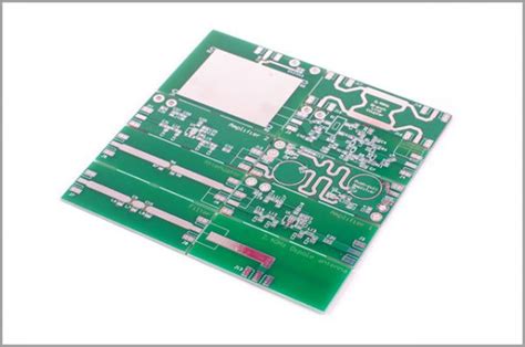
PCB Panelization Guidelines
When preparing PCB designs for panelization, following some best practices helps ensure good manufacturing results:
Breakaway Tabs
Including breakaway tabs (also known as mouse bites) between boards allows them to be cleanly snapped apart after production. The tabs should be strong enough to hold during handling but not so thick that depanelization is difficult. Typical tab sizes are:
| Tab Type | Recommended Size |
|---|---|
| V-groove | 0.3 – 0.7 mm |
| Perforated | 1.0 – 1.5 mm |
Tooling Holes and Fiducials
Adding tooling holes and fiducials to the panel allows automated assembly machines to accurately locate and process the boards. Two 2-3mm tooling holes are typically drilled near diagonally opposite corners. At least 3 fiducial marks, ideally one near each corner, should be included on the panel. The fiducial marks should be copper pads without soldermask about 1mm in diameter.
Rail Spacing
Ensuring adequate rail spacing around the edge of the panel provides room for handling and reduces warpage risk. Ideally, the space between the edge of the panel and any board features should be:
| Panel Thickness | Recommended Rail Width |
|---|---|
| <0.8 mm | 5 mm |
| 0.8 – 1.2 mm | 7 mm |
| 1.2 – 2.0 mm | 10 mm |
Testing Coupons
Including a test coupon on the panel allows the bare board to be tested for manufacturing quality before assembly. The coupons usually contain patterns for probing things like:
- Solder bridging
- Minimal trace/space
- Plated hole size and annular ring
- Dielectric strength

PCB Depanelization Methods
After assembly, individual boards need to be depanelized from the manufacturing panel. Common depanelization methods include:
V-Groove
V-groove depanelization uses a special V-shaped blade to cut 30-50% through the panel, creating a weak spot where it can be broken apart. This method is commonly used for thinner 0.8-1.0 mm boards.
Tab Routing
Tab routing leaves small tabs attaching the boards to the frames. After assembly the tabs can be cut or broken to remove the individual PCBs. This tends to be used for boards thicker than 1.0mm.
Perforated Lines
Perforated mousehole patterns can be drilled or routed along the board edges so they can be easily snapped apart later.

FAQ
1. What is the minimum spacing between boards on a panel?
For V-groove depanelization, there should be at least 0.3mm between the edge of any board and the tabs. For perforated or routed tabs, 1.5-2.0mm space is recommended.
2. How thick can PCB panels be?
Most PCB manufacturers can fabricate and panelize boards up to 3-4mm thick. The thickness is limited by the mAXImum depth of the cutting tools.
3. What is the typical PCB panel size?
The most common panel sizes are 9×12 inch (229x305mm), 12×18 inch (305x457mm), and 18×24 inch (457x610mm). Larger 21×24 inch panels are sometimes used for high volume production.
4. Can different PCB designs be panelized together?
Yes, as long as the different designs use the same stackup, material, thickness, and other specifications, they can be mixed on a panel. This is often done for boards going into the same product.
5. What does PCB panelization cost?
The cost of PCB panelization depends on the size and complexity of the panel design and the fabrication specifications. However, the panelization cost is typically very low compared to the full cost of manufacturing the PCBs themselves. Simple panelization is often included for free or just a few dollars per panel by most manufacturers.
In summary, PCB panelization is an important step in the PCB manufacturing process that allows multiple boards to be efficiently and consistently fabricated together. By grouping boards onto panels with tooling holes, fiducials, and breakaway tabs, the individual PCBs can be smoothly produced in volume and then depanelized after assembly. Knowing the guidelines and best practices for panelization helps ensure successful, high-quality results.
Leave a Reply