Introduction to PCB Stack-Up Design
Printed Circuit Board (PCB) stack-up refers to the arrangement of copper and insulating layers that make up a PCB. The stack-up design is a critical aspect of PCB design as it directly impacts the electrical performance, manufacturing process, and overall cost of the final product. A well-designed PCB stack-up ensures proper signal integrity, reduces electromagnetic interference (EMI), and enhances the reliability of the PCB.
In this article, we will discuss eight essential rules for designing an effective PCB stack-up. By following these guidelines, you can create a robust and reliable PCB that meets your design requirements.
Rule 1: Determine the Number of Layers
The first step in designing a PCB stack-up is to determine the number of layers required for your design. The number of layers depends on various factors such as the complexity of the circuit, the number of components, signal integrity requirements, and manufacturing constraints.
Here are some general guidelines for choosing the number of layers:
| Number of Layers | Application |
|---|---|
| 1 or 2 | Simple designs with low component count and low-speed signals |
| 4 | Most common, suitable for moderate complexity and speed |
| 6 or 8 | Complex designs with high component density and high-speed signals |
| 10 or more | Very complex designs with extremely high-speed signals and dense routing |
Keep in mind that increasing the number of layers also increases the manufacturing cost and complexity. Therefore, it is essential to strike a balance between the design requirements and cost-effectiveness.

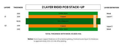
Rule 2: Choose the Appropriate Layer Stack-Up
Once you have determined the number of layers, the next step is to choose an appropriate layer stack-up. The layer stack-up defines the arrangement of signal, power, and ground layers within the PCB.
A typical 4-layer PCB stack-up might look like this:
| Layer | Description |
|---|---|
| Top | Signal layer |
| Inner | Ground layer |
| Inner | Power layer |
| Bottom | Signal layer |
In this arrangement, the signal layers are placed on the outer layers to minimize the dielectric thickness and improve signal integrity. The ground and power layers are placed on the inner layers to provide shielding and reduce EMI.
For higher layer counts, you can alternate signal and plane layers to maintain a symmetrical stack-up. This helps to minimize warpage and ensures better manufacturability.

Rule 3: Define the Layer Thicknesses
The thickness of each layer in the PCB stack-up plays a crucial role in determining the electrical characteristics and manufacturability of the board. The layer thicknesses should be chosen based on the desired impedance, current carrying capacity, and manufacturing constraints.
Here are some common layer thicknesses used in PCB design:
| Layer | Thickness (mil) |
|---|---|
| Copper | 0.5 – 2.8 |
| Core | 4 – 8 |
| Prepreg | 2 – 4 |
| Solder Mask | 0.5 – 1.0 |
| Silkscreen | 0.2 – 0.3 |
The copper thickness determines the current carrying capacity of the traces. Thicker copper layers can handle higher currents but also increase the overall thickness of the board. The core and prepreg thicknesses affect the dielectric constant and impedance of the board. Solder mask and silkscreen thicknesses are chosen based on the manufacturing process and component labeling requirements.

Rule 4: Consider the Dielectric Material
The choice of dielectric material is another important factor in PCB stack-up design. The dielectric material is the insulating layer between the copper layers and affects the electrical properties of the board.
Common dielectric materials used in PCB manufacturing include:
- FR-4: Most widely used, cost-effective, and suitable for general-purpose applications
- Rogers: High-performance material with low loss and stable dielectric constant, ideal for high-frequency and RF applications
- Polyimide: High-temperature resistant material with excellent mechanical and electrical properties, suitable for aerospace and military applications
The dielectric constant (Dk) and loss tangent (Df) of the material determine the signal propagation speed and loss in the PCB. A lower Dk results in faster signal propagation, while a lower Df reduces signal attenuation.
Rule 5: Maintain Consistent Impedance
Maintaining consistent impedance throughout the PCB is crucial for ensuring signal integrity and reducing reflections. The impedance of a trace depends on its width, thickness, and the properties of the surrounding dielectric material.
To maintain consistent impedance, follow these guidelines:
- Use controlled impedance design techniques, such as microstrip or stripline, for critical signals
- Keep the trace width and spacing consistent within a layer
- Avoid abrupt changes in trace geometry, such as sharp bends or transitions between layers
- Use impedance matching techniques, such as termination resistors or stubs, to minimize reflections
Impedance control is particularly important for high-speed signals, such as clock lines, memory interfaces, and high-speed serial links.
Rule 6: Minimize Cross-Talk and EMI
Cross-talk and electromagnetic interference (EMI) can degrade signal quality and cause system malfunctions. To minimize these effects, consider the following guidelines in your PCB stack-up design:
- Separate sensitive signals from noisy signals by placing them on different layers or using guard traces
- Use ground planes or power planes to provide shielding between layers
- Route high-speed signals on inner layers, sandwiched between ground planes, to minimize radiation
- Use differential signaling for high-speed interfaces to cancel out common-mode noise
- Avoid routing signals parallel to each other for long distances to reduce coupling
Proper grounding and shielding techniques can significantly reduce cross-talk and EMI in your PCB design.
Rule 7: Plan for Manufacturing and Assembly
When designing your PCB stack-up, it is essential to consider the manufacturing and assembly processes. Some key factors to keep in mind include:
- Minimum trace width and spacing: Ensure that your design meets the manufacturer’s guidelines for minimum trace width and spacing to avoid fabrication issues
- Copper balance: Maintain a similar amount of copper on each layer to prevent warping during the manufacturing process
- Via size and spacing: Choose appropriate via sizes and spacing based on the manufacturer’s capabilities and design requirements
- Solder mask and silkscreen: Include solder mask and silkscreen layers in your stack-up for proper insulation and component labeling
Consulting with your PCB manufacturer early in the design process can help you avoid potential manufacturing issues and optimize your stack-up for production.
Rule 8: Document and Communicate Your Stack-Up
Finally, it is crucial to document and communicate your PCB stack-up design to all stakeholders, including the design team, manufacturers, and assemblers. A clear and well-documented stack-up helps to ensure that everyone involved in the project has a common understanding of the design intent and requirements.
Your stack-up documentation should include:
- A visual representation of the layer arrangement, including layer names, thicknesses, and materials
- A table with the detailed specifications of each layer, such as copper weight, dielectric constant, and impedance targets
- Notes on any special requirements, such as controlled impedance or high-voltage clearances
- Revision history and approval signatures
Maintaining accurate and up-to-date stack-up documentation is essential for successful PCB design and manufacturing.
Conclusion
Designing an effective PCB stack-up is a critical aspect of PCB design that directly impacts the performance, reliability, and manufacturability of the final product. By following the eight rules discussed in this article, you can create a robust and well-optimized PCB stack-up that meets your design requirements.
Remember to consider factors such as the number of layers, layer arrangement, dielectric materials, impedance control, cross-talk and EMI reduction, manufacturing constraints, and proper documentation. By taking a holistic approach to PCB stack-up design, you can ensure the success of your PCB project.
Frequently Asked Questions (FAQ)
1. What is the most common number of layers in a PCB stack-up?
The most common number of layers in a PCB stack-up is four. A 4-layer PCB provides a good balance between design complexity, signal integrity, and cost-effectiveness for many applications.
2. What is the purpose of ground and power planes in a PCB stack-up?
Ground and power planes in a PCB stack-up serve multiple purposes:
- They provide a low-impedance return path for signals, reducing loop area and minimizing EMI
- They offer shielding between layers, reducing cross-talk and improving signal integrity
- They distribute power efficiently to components across the board
3. What is controlled impedance, and why is it important in PCB design?
Controlled impedance refers to the practice of designing PCB traces with a specific target impedance to ensure proper signal integrity. It is important in PCB design because:
- It minimizes signal reflections and distortions, especially for high-speed signals
- It ensures proper termination and matching between the source, trace, and load
- It helps to maintain signal quality and timing integrity throughout the system
4. How does the choice of dielectric material affect PCB performance?
The choice of dielectric material in a PCB stack-up affects several aspects of performance:
- The dielectric constant (Dk) determines the signal propagation speed and wavelength in the material
- The loss tangent (Df) determines the amount of signal attenuation and power dissipation in the material
- The thermal and mechanical properties of the material affect the PCB’s ability to withstand stress and heat
Choosing the right dielectric material based on the application requirements is crucial for optimizing PCB performance.
5. What are some common issues that can arise from improper PCB stack-up design?
Some common issues that can arise from improper PCB stack-up design include:
- Signal integrity problems, such as reflections, cross-talk, and distortions
- Electromagnetic interference (EMI) and radio frequency interference (RFI)
- Manufacturing issues, such as warping, delamination, or difficulty in fabrication
- Reliability issues, such as thermal stress, mechanical stress, or moisture ingress
By following best practices and guidelines for PCB stack-up design, you can minimize these issues and ensure the optimal performance and reliability of your PCB.
Leave a Reply